


neskor
-
Broj sadržaja
2861 -
Na DiyAudio.rs od
-
Poslednja poseta
-
Broj dana (pobeda)
34
Content Type
Profiles
Forum
Blog
Kalendar
Sve objavljeno od neskor
-
Ne radi se o samo jednoj plocici, ima 6 razlicitih plocica za razlicite namene. Nasao sam na netu uputstvo kako sa Kicad-om odraditi drilling files, tako da sam to danas i resio Milsio sam da ce biti mnogo komplikovano ali na srecu nije tako bilo. Svaki dan se nauci nesto novo Hvala svima na pomoci!
-
hajde da pokusam ja da uradim sam, nasao sam neki totorijal na netu pa ako ne uspem javljam hvala puno za pomoc!
-
nemam pojma, to sam dobio u zip fajlu tako da ne znam koji je izvorni program velicine rupa mogu da se vide sa slike koji je inace standard za rupe na PCB-u za otpornike?
-
Imam neke zip gerber fajlove koje treba da izradim on jlpcb, medjutim kazu mi da mi fale "drill file". Da li ima neko voljan da mi to doda ili da mi posalje uputstvo ili link kako da to dodam. Na slikama imam te rupe, ali nazalost u gerber zip fajlu ga ne vidim U prilogu je samo jedan zip file i slika tog pcb-a, ukupno ih imam 6. Reley 2 pcb.BMP Reley 2.zip
-

Zanimljive, smešne i čudne fotografije
neskor je odgovorio/la Mikorist's temus u Muzika , Film i Fotografija
-
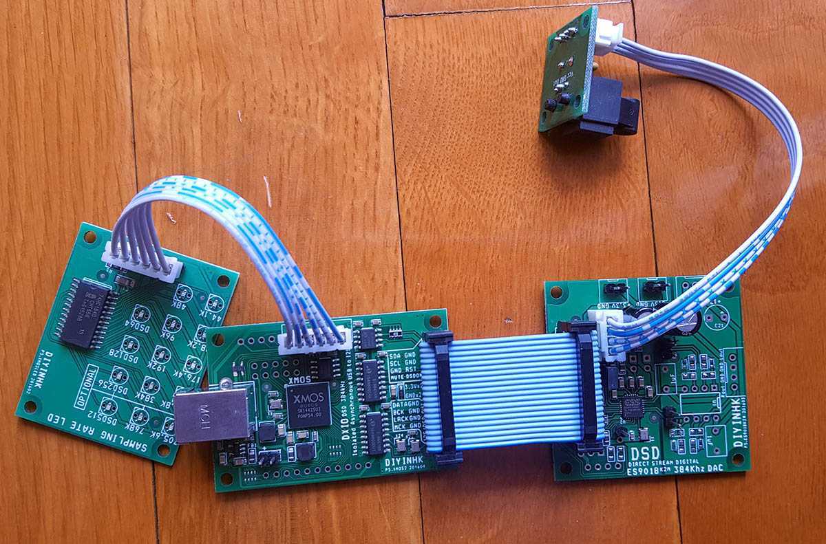
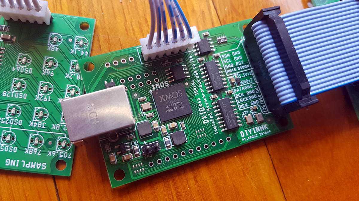
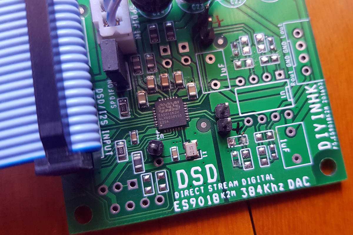
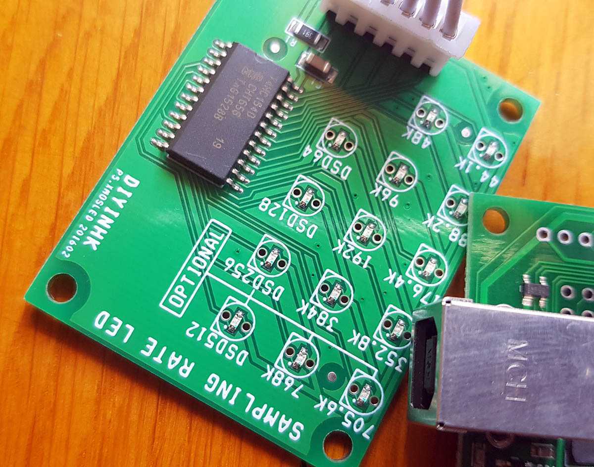
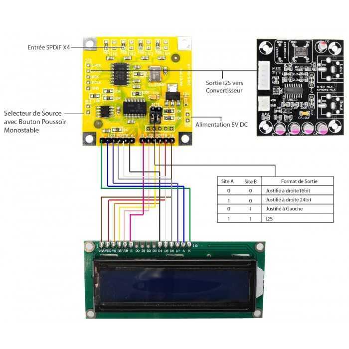
evo i link za DAC board https://www.diyinhk.com/shop/audio-kits/114-usb-dsd-dxd-384khz-dac-with-bit-perfect-volume-control-and-spdif-inputxmoses9018k2m.html#/dac-xmos_384k_isolated_dac_and_led_pcb
-
verovatno nemate pristup posto je google drive 'ajmo onda ovako

-
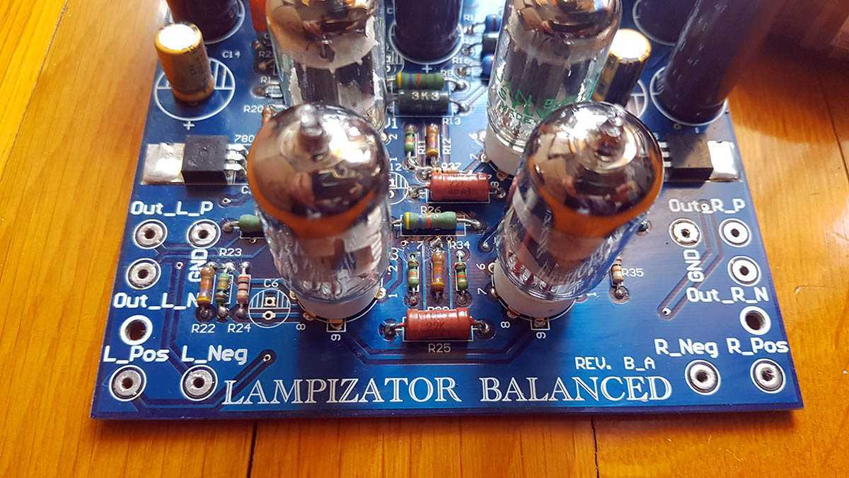
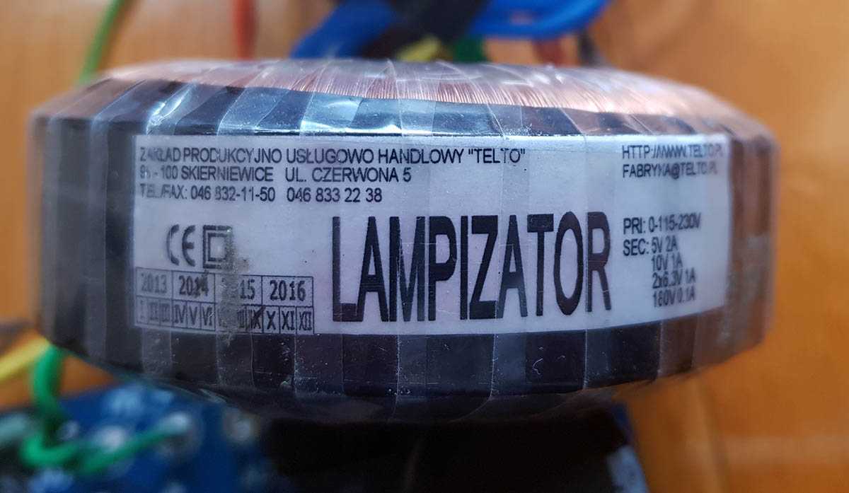
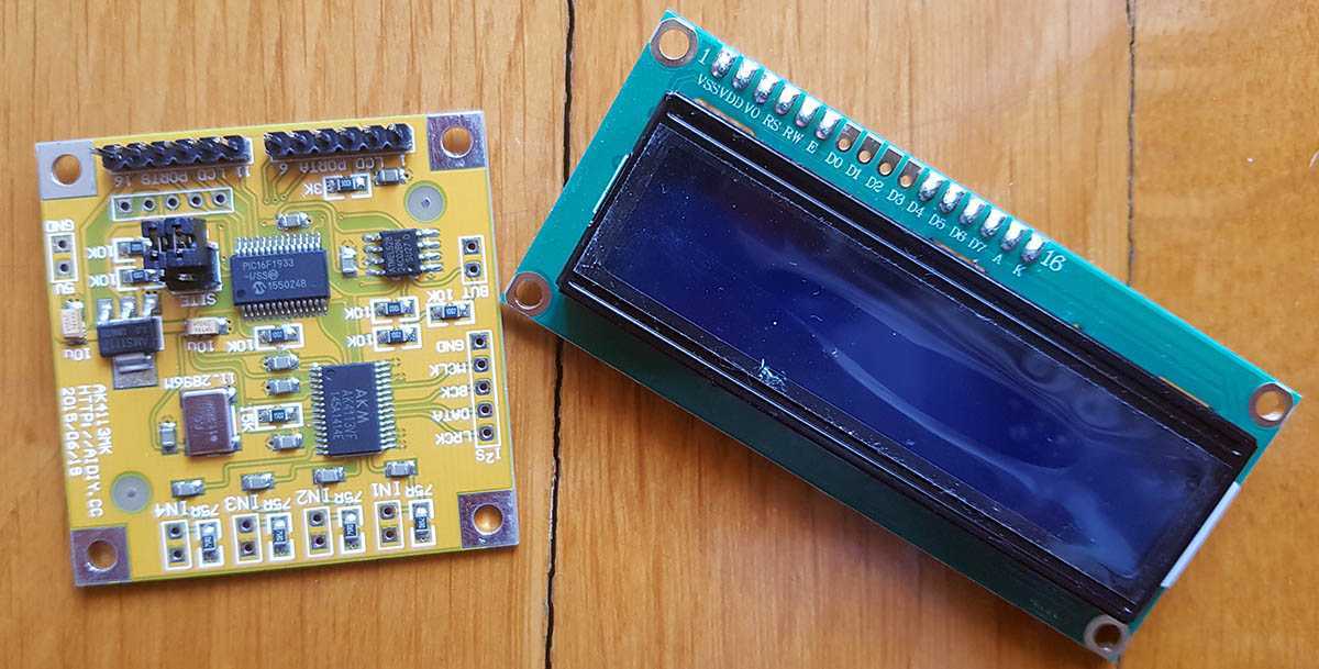
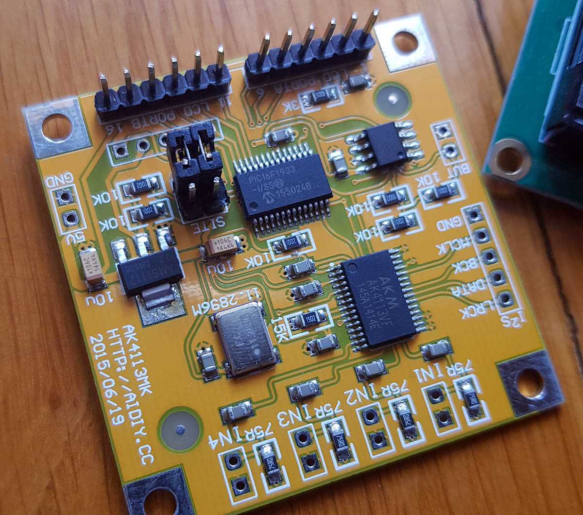
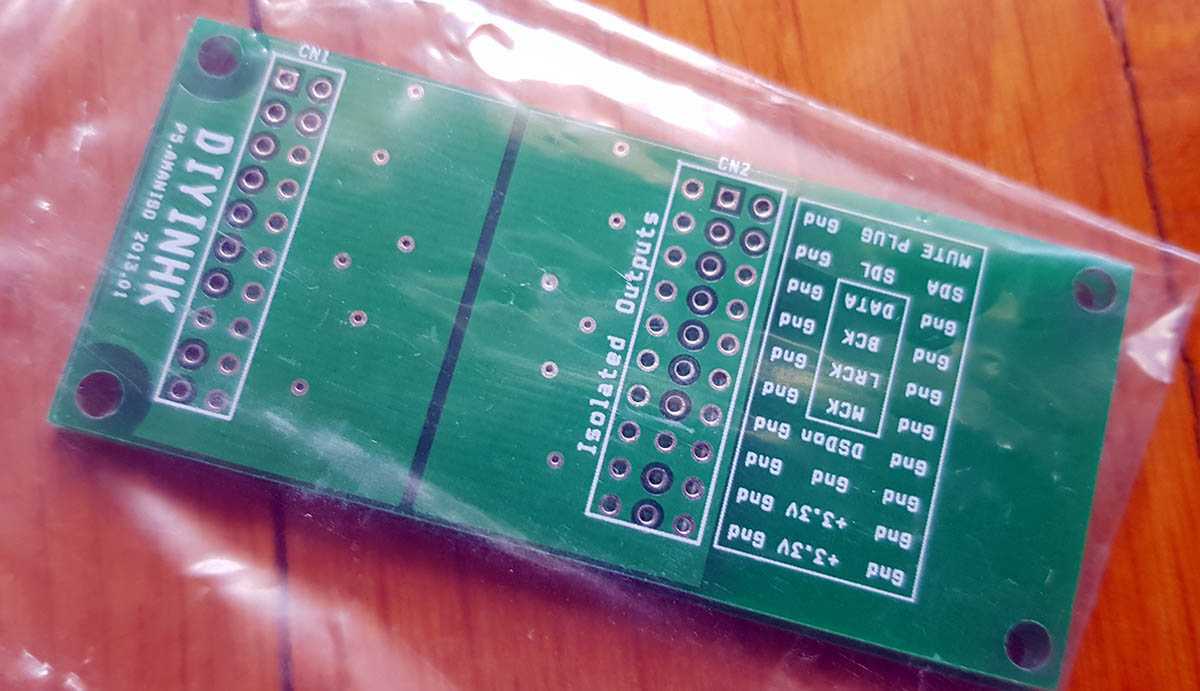
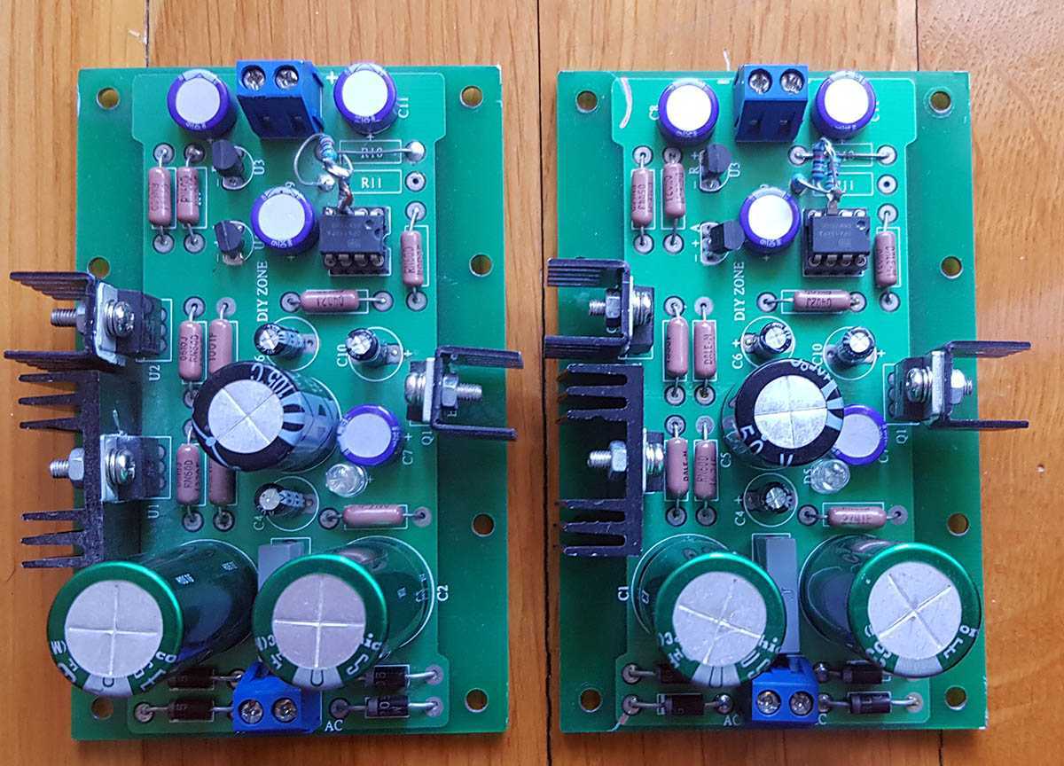
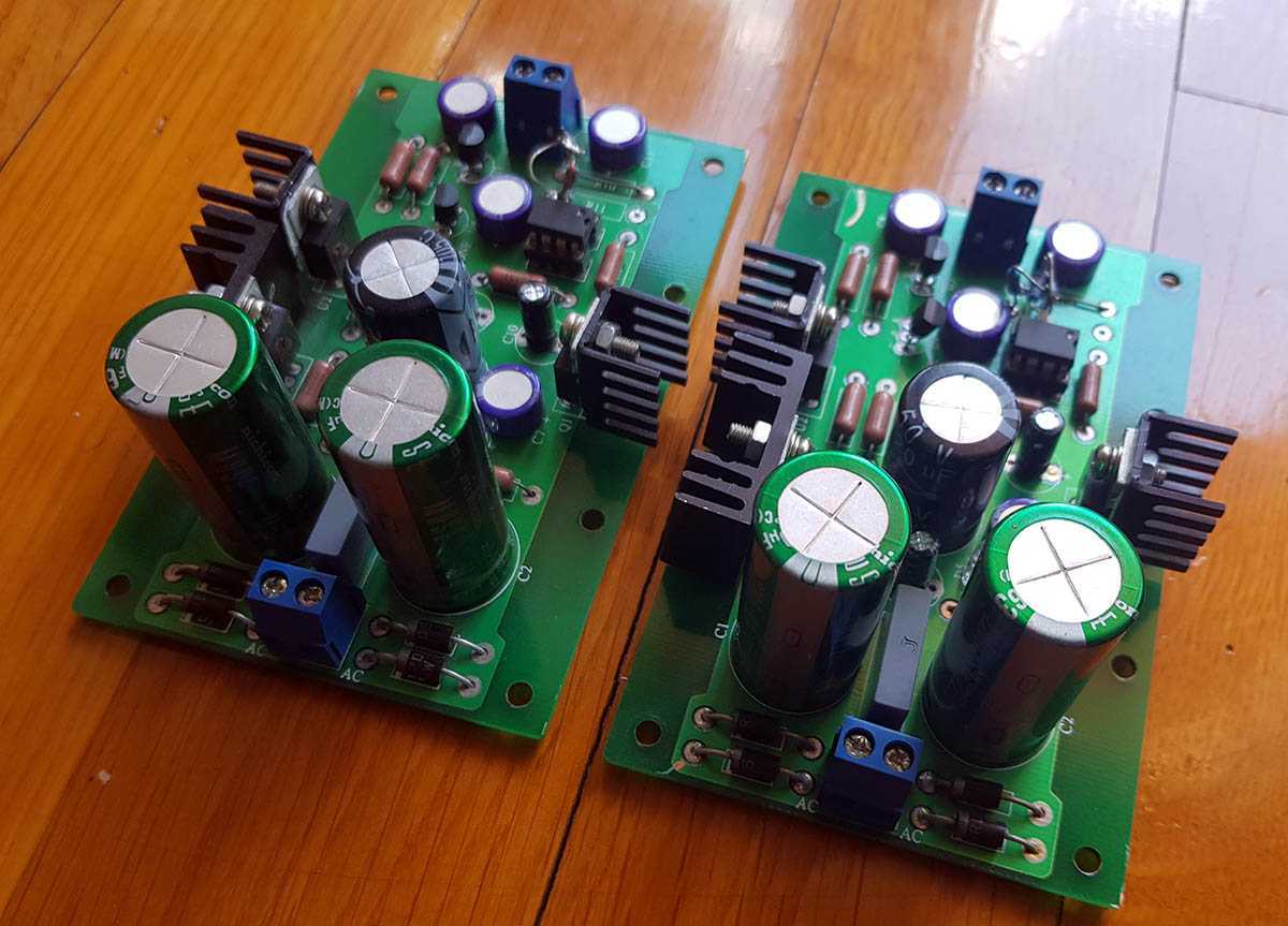
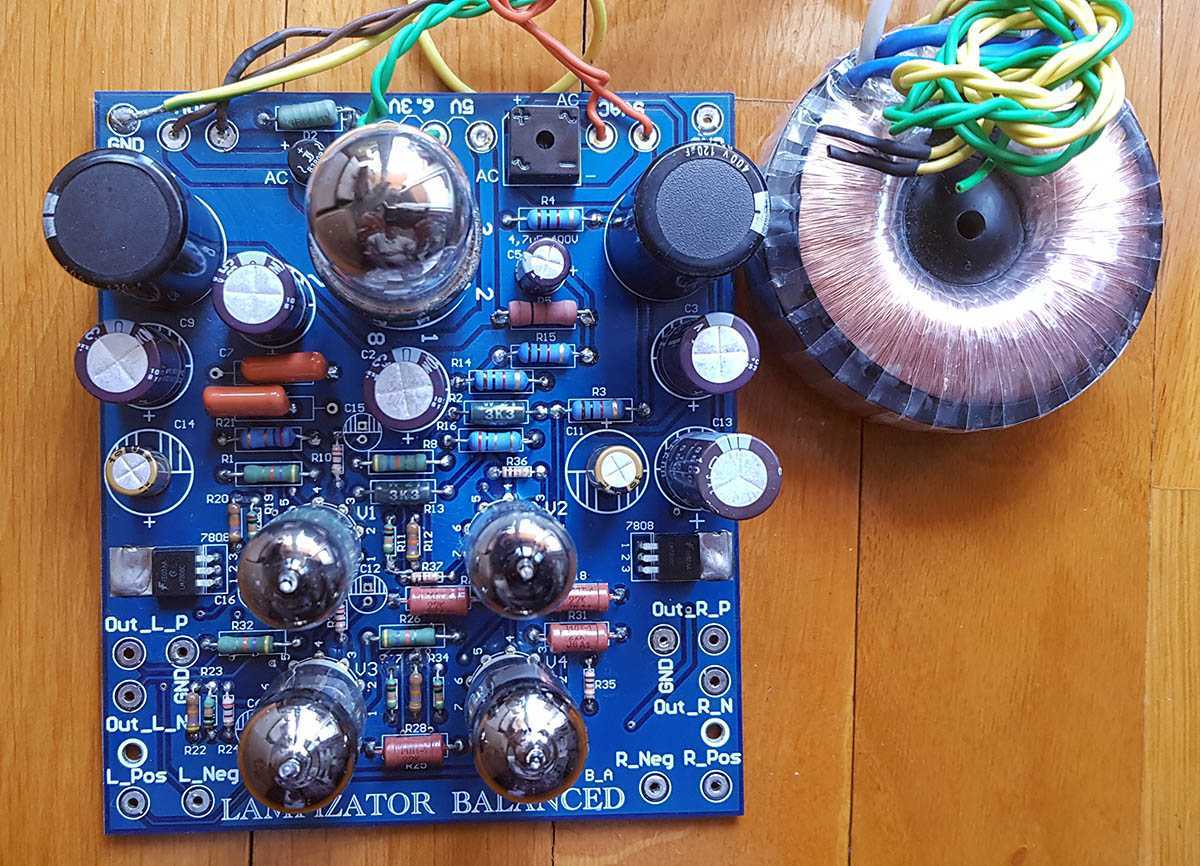
Prodajem Lampizator Amber Balanced KIT. Kupio sve delove sa mislju da uradim kopiju mog Lampizatora Amber ali u balansiranoj verziji i odustao. Svi delovi su to potrebni da se napravi kompletan DAC, kao i tehnicka pomoc Lampizator Amber Balanced PCB Trafo: AK4113 Digital receiver board SPDIF to I2S converter software control + LCD DIYINHK XMOS USB to i2s + ES9018K2M DAC DIYINHK i2s izloator Napajanje 3,3V i 5V Cena za forum je 500 EUR za sve, ovakav fabricki dac je reda 2K EUR.
-
gde si uzeo taj mali UNI-T generator?
-
3H ima da se nadje za nekih 16K dinara
-
dobro dosao u klub, imam ga i ja
-
tako sam i pretpostavio, onda bolje to ostaviti profesionalcima
-
bilo je i ranije, ali sam mislio da nesto rezonira u pojacalu ili samoj prostoriji sada kada sam ih izvadio iz pojacala video sam da oni prave problem inace zvucnici probani na tri pojacala i na svakom je isto, takodje proba to staro pojacalo sa novim zvucnikom i nema tog problema ti zvucnici su dosta stari i verovatno je sam kartom i vesanje ostarilo, pa sam zato pomislio sa ako ih premazem sa nekom tecnoscu da cu im vratiti elasticnost
-
nije definitivno to, probao sada opet i cuje se to treperenje cim sviram na zadnjoj zici niske tonove
-
drajveri su izvuceni iz kutija i onda testirani to je i meni prvo bila ideja
-
sada sam izmerio i FS se krece od nekih 120Hz do 150Hz mislim da to treperenje membrane nema toliko veze sa Fs takodje proverio pletenice i sve ostale delove i ne vidim da bilo sta cese
-
Zadnih par meseci sam primetio da mi pojacalo za gitaru proizvodi cudne zvuke na bas frekvencijama. Mislio sam da nesto unutar pojacala nije dobro stegnuto pa vibrira, medjutim ustanovio sam da su problem zvucnici. Ne odredjenoj bass frekvenciji prozivode zujanje, tacnije kao da papir membrane cese o nesto. Pustio sam zvuznike na ton generator i ustanovio da je kalem dobro centriran i da tu nista ne cese, medjutim na oko 90Hz cuje se treperenje membrane. Mene sada zanima da li je tu nesto moguce uraditi. Da li ce pomoci ako se vesanja premazu, ili cak cela membrana? Zvucnik je Fender CTS od 10", imam 4 komada i svi se ponasaju slicno. Probao sam i na drugom pojacalu ali opet ista situacija. Evo i slike zvucnika ( slika sa neta)
-
Zanimljive, smešne i čudne fotografije
neskor je odgovorio/la Mikorist's temus u Muzika , Film i Fotografija
-
mene vise zacudi kada nesto ima u Srbiji, nego kada nema
-
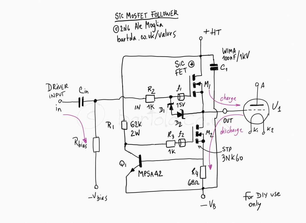
evo sheme i SF PCB
-
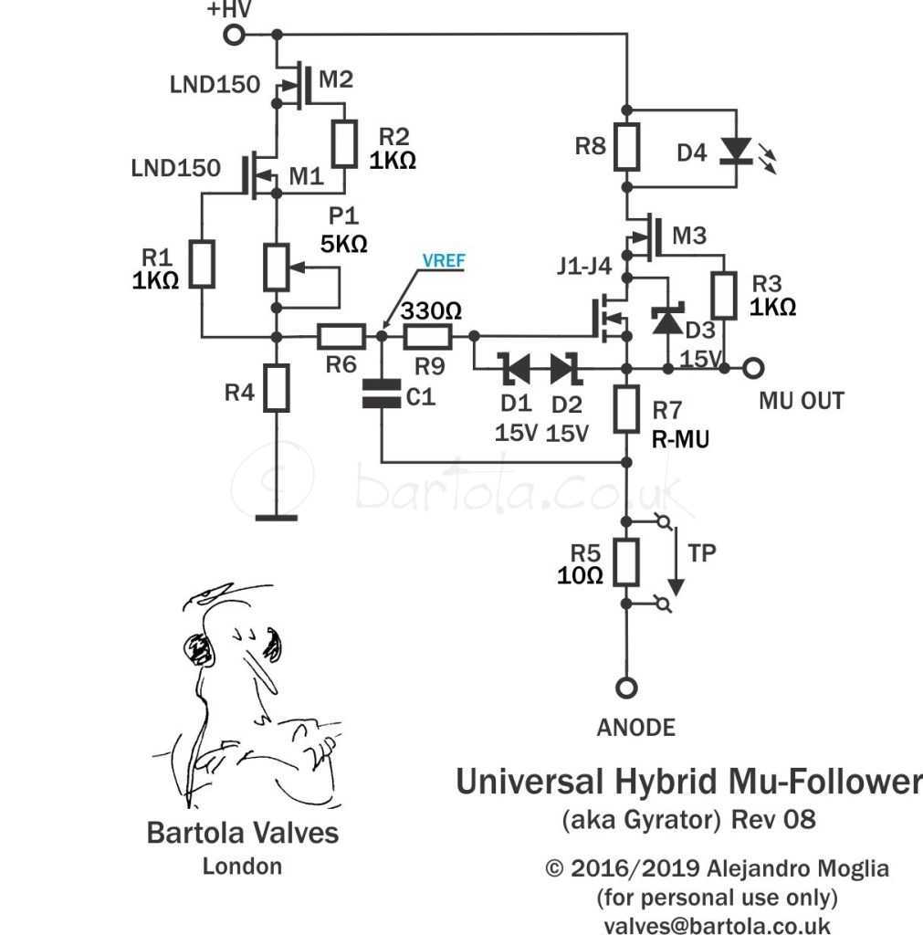
The circuit is very simple. The depletion MOSFET pair M1 and M2 (LND150) forms an CCS. This CCS provides a stable current to develop a reference voltage across R4 for the gyrator. This voltage will bias the cascoded pair J1-3 and M3 through R6. D1, D2 and D3 protect J1-3. R5 is simply a test resistor to measure the anode current. R7 is the mu resistor which is optimized for each stage. C1 provides the bootstrapping needed for AC operation and achieve the low output impedance in the mu output. The top depletion MOSFET (M3) does all the heavy lifting. For low currents (e.g. 1-10mA) it doesn’t need a heatsink, however when the gyrator is used in a driver or when currents are greater than 10mA you’d expect to put a small TO-220 clip-on heatsink or bolt it to chassis if needed. The low frequency response is primarily driven by the RC pair R6 and C1. Typically, I’d use the following combinations: 4.7MΩ and 220nF or 10M and 100nF. The high frequency response is driven by the parasitic capacitances of the lower FETs. Therefore, you want to use a low-noise jFET in J1-3 instead of another depletion FET (unless it has low reverse capacitances – see the BOM and appendix section for more details). The jFET on this position is operating in very unfavorable conditions (i.e. low drain-source voltage) so best use a jFET here for best results. The circuit has minimum protection and if you short accidentally any output you will kill M3 and J1-3 for sure. The voltage reference is pretty resilient, though, however it can be damaged as well. For the lower FET protection, you will need to add three 15-18V Zener diodes (D1-D3). This is covered later in more detail in the build section. The value of R4 is determined by the optimal CCS current needed by the LND150 devices for best temperature compensation. This is about 500uA, so the value of R4 is roughly the output voltage divided this reference current.
-
https://www.bartola.co.uk/valves/2018/04/28/hybrid-mu-follower-output-impedance/
-
evo i sheme Gyrator-a
-
Sta god da napravite od ovoga necete zazaliti https://www.bartola.co.uk/valves/2021/02/06/the-low-gain-dht-pre-amp-library/
-
ima ovde par smernica https://www.diyaudio.com/forums/solid-state/179004-luxman-357-schematic.html i kazu da je shema slicna sa A 383 tu semu imas ovde: https://www.vintageshifi.com/repertoire-pdf/Luxman.php


-
Trenutno na sajtu 3 članova, 0 Skrivenih, 105 Gosta (Pogledaj celu listu)
-
Forumska statistika
9.2k
Ukupan broj tema452.2k
Ukupan broj objava