

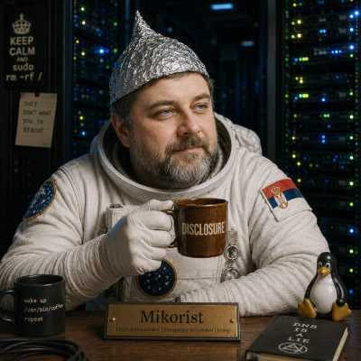
Mikorist
-
Broj sadržaja
46954 -
Na DiyAudio.rs od
-
Broj dana (pobeda)
654
Content Type
Profiles
Forum
Blog
Kalendar
Sve objavljeno od Mikorist
-
Prevod ebo bambulu ja prevodoh.......... titl.srt
-
Još Ko ima Televizor od par metara - Gušt...samo viski sa ledom
-
Procureo Dune skriner neciji na 1337x.........jbg
-
Zašta će tebi ovo ? Ovo stavljaju ameri u brojila da nemož magnet da zvekneš
-
-
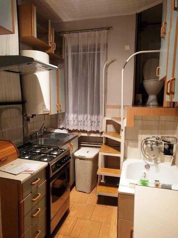
Zanimljive, smešne i čudne fotografije
Mikorist je odgovorio/la Mikorist's temus u Muzika , Film i Fotografija

-
-
Ovde bre ima celo takmičenje u demixingu da vidite samo koja matematika stoji iza ovoga https://www.aicrowd.com/challenges/music-demixing-challenge-ismir-2021
-
Ako nekom treba da iščupa vokal iz muzike https://github.com/deezer/spleeter pip install spleeter ovako odvaja ~/.local/bin/spleeter separate -p spleeter:2stems -o output 0000.flac Bokte mazo kako ovo radi... primer p.s. Tražim ovo godinama - i ovo je naj što postoji do sad.
-
još jedan fenomen
-
-
On jeste ....Ili Sigrid jbt
-
Jok ja....Dodatni magneti peglaju to. A možeš i dodatno da se zezaš sa dampingom pozadi. Ama samo sa magnetima to peva ubija. Dal samo magnetno polje, dal masa dodatna - za te pare nema bolje....
-
-
-
Fetiš......... Za mene recimo sve od 12 - 15 inča - Extended-Range - ima mistični kvalitet . Trubice koncentičnih oblika - fazni čepovi od drške od lopate Vudu bajo
-
sve je to super - ali IEC mu pogledaj D'Agostino veliki stručnjak za amperažu. Da li je nekad u životu video kako izgledaju muški i ženski priključcii za 40A i kabl... Ili šasijski na 40A
-
Jedno ali obrnuto ∀
-
Pa ne može niko da stavi profit ispred nacionalne bezbednosti USA. Već jednom je imao sipitivanje na tu temu i kleo se pred senatom da će sve da bude u redu. Onda kad je bio slučaj sa Cambridge Analytica - tad je imao prvu ličnu........Posle toga su olavbavili algoritam (i uzeli gomilu love od Trampa) i kad je puklo sa onim događajem sa Trampom - to mu je druga lična (bez obzira što su banovali Trampa ). Nakon toga poslali su insajdera u sam Fejsbuk - ovu uzbunjivačicu da ispita da li su normalni. Sad je dobio crveni karton...Plus sav prljav veš je isplivao napolje....Ako neko misli da ona ne radi za NSA grdno se vara...Šta će duboka država da radi naknadno to ostaje da se vidi.
-
Pogledajte optužbe uzbunjivačice - i zaključke senata. 1. Fejsbuk ne može da nastavi da radi sam bez pomoći spolja - a da ne ugrozi bezbednost nacionalnu. 2. Sva istraživanja koja su radili interno moraju javno da budu objavljena u skladu sa tačkom 1 - i njih moraju da prate naučni timovi van Fejsbuka - regulatorno telo. 3. Zakerberg ne ume sam da vodi kompaniju bez pomoći spolja
-
Ali pogledaj Zakerbergovo saslušanje od strane kongresa. Svaka druga reč mu je nemam pojma - nisam upoznat i moram da se konsultujem sa timom o toj stvari. Čak i na pitanje o alatu za praćenje i moderaciju korisnika. Ili je senilan ili se pravi lud ili laže. Za laganje pred senatom je zaprećena kazna zatvororm....


-
Trenutno na sajtu 1 član, 1 Skrivenih, 443 Gosta (Pogledaj celu listu)
-
Forumska statistika
9.2k
Ukupan broj tema452.1k
Ukupan broj objava -
Statistika članovȃ
3017
Svi članovi5071
Najviše na sajtu