

Mikorist
-
Broj sadržaja
46523 -
Na DiyAudio.rs od
-
Broj dana (pobeda)
626
Content Type
Profiles
Forum
Blog
Kalendar
Sve objavljeno od Mikorist
-
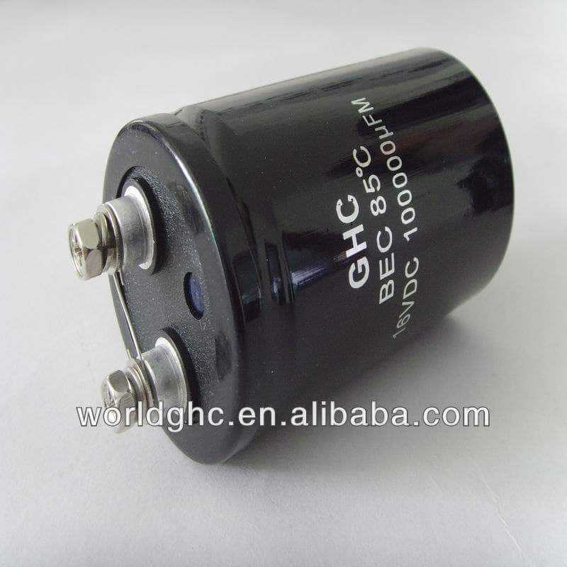
Problem je i veličina. 25cm je dužina a 10cm širina
-
https://www.alibaba.com/product-detail/25v-1f-capacitor-electrolytic-with-high_1580848259.html?spm=a2700.7724857.normalList.2.395053d63Yg8MT pa puta 8 u pojačalu... 8 Farada

-

Zanimljivi & smešni na You Tube
Mikorist je odgovorio/la Leonardo's temus u Muzika , Film i Fotografija
Ali deo gde kaže da jedina savršena reprodukcija jeste da se snima električni impuls mozga koji sluša čelo uživo i potom da se putem elektroda reprodukuje u drugom mozgu. -
Zanimljivi & smešni na You Tube
Mikorist je odgovorio/la Leonardo's temus u Muzika , Film i Fotografija
-
Oni u Mekintošu vakumiraju i stavljaju to crno u konzervu. Pa peku - suše u peći sve zajedno. A konzerva je 4mm bakar. glavna caka je je u vakuumupumpi
-
ma treba uverenje od drugog doktora... za glavu.... celo pojačalo od bakra kao bakrač a audiofil čuje deo od 1cm pozlaćen u bakraču...
-
Oću da kažem da svaki deo treba da je ultimativan. I postolje za osigurač...I štampana pločica mora da je pure gold... Inače plemeniti metali (samo po periferiji) ne piju vodu...
-
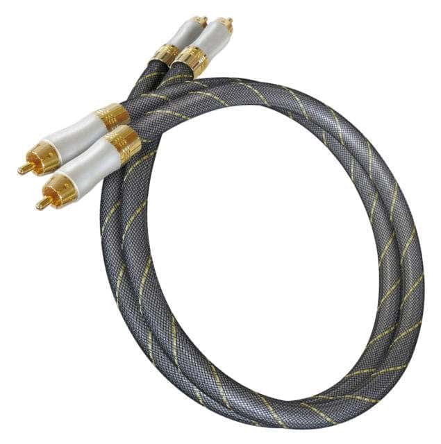
pa džaba osigurač od 45 evra ako je postolje od osigurača 0.5 evra.... isto kao što je džabe kabl od 200 evra koji samo 0.5 mikrona ima pozlatu na telu od RCA koji je od bronze
-
šta fali DYNAVOX-u ? 40 evra kabl...
-
Zanimljive, smešne i čudne fotografije
Mikorist je odgovorio/la Mikorist's temus u Muzika , Film i Fotografija
-
Zanimljive, smešne i čudne fotografije
Mikorist je odgovorio/la Mikorist's temus u Muzika , Film i Fotografija
"Doći će žuti ljudi i restauriraće spomenik..."
-
Onda da ne brinem što Sissy ima samo 18W ako slušam na zvučnicima od 94db
-
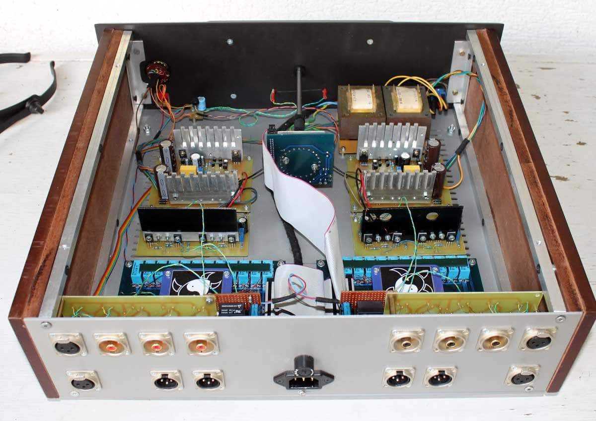
za OVO ide ovako nešto - veće duplo od Hirage. Ko trafo stanica rođaci.
-
Teško da će ispravljač od laptopa da uspe da pogura struju dovoljnu za zvučnik sem onog od kompa. Meni ova minika i izgleda kao pc pojačalo.
-
Vidiš da čekaju da se usvira. Pametni ljudi... ^ A ne kao neki koji probaju pojačalo odma neusvrano i daju ocene (plus što im je i predpojačalo jadno - bar 5 cenovnih klasa ispod probanog uređaja) ....
-
Zanimljivi & smešni na You Tube
Mikorist je odgovorio/la Leonardo's temus u Muzika , Film i Fotografija
tek sad vidim koliko je veliki ovaj BUSTER koji vertikalno sleće...... bokte -
-
Ma jok. Kad već prednjice idu kod tebe , klirit, dugmad, graviranje, ide i 8 stopa u kompletu.... One prošle su bile haj-end... nego ne mogu da ih nađem... Pa bude 8. Nego razmišljam dal i zadnjicu da šaljem na graviranje..... za Pumpkina Ko će da se snađe sa 14 Neutrika
-
Ja kod @Leonardo naručujem nogice. I za amp i za preamp....Mislim da nema bolje.
-
Zanimljive, smešne i čudne fotografije
Mikorist je odgovorio/la Mikorist's temus u Muzika , Film i Fotografija
-
Zanimljive, smešne i čudne fotografije
Mikorist je odgovorio/la Mikorist's temus u Muzika , Film i Fotografija
-
-
https://www.zenbotcnc.com/ nova makina za @Leonardo
-
For Sissy SIT
-
PSYTrance , HoUsE, TEChNO, eLeCtRo, AmBienT :)
Mikorist je odgovorio/la BANAT's temus u Muzika , Film i Fotografija


-
Trenutno na sajtu 2 članova, 1 Skrivenih, 227 Gosta (Pogledaj celu listu)
-
Forumska statistika
9.1k
Ukupan broj tema450.7k
Ukupan broj objava -
Statistika članovȃ
3006
Svi članovi5071
Najviše na sajtu